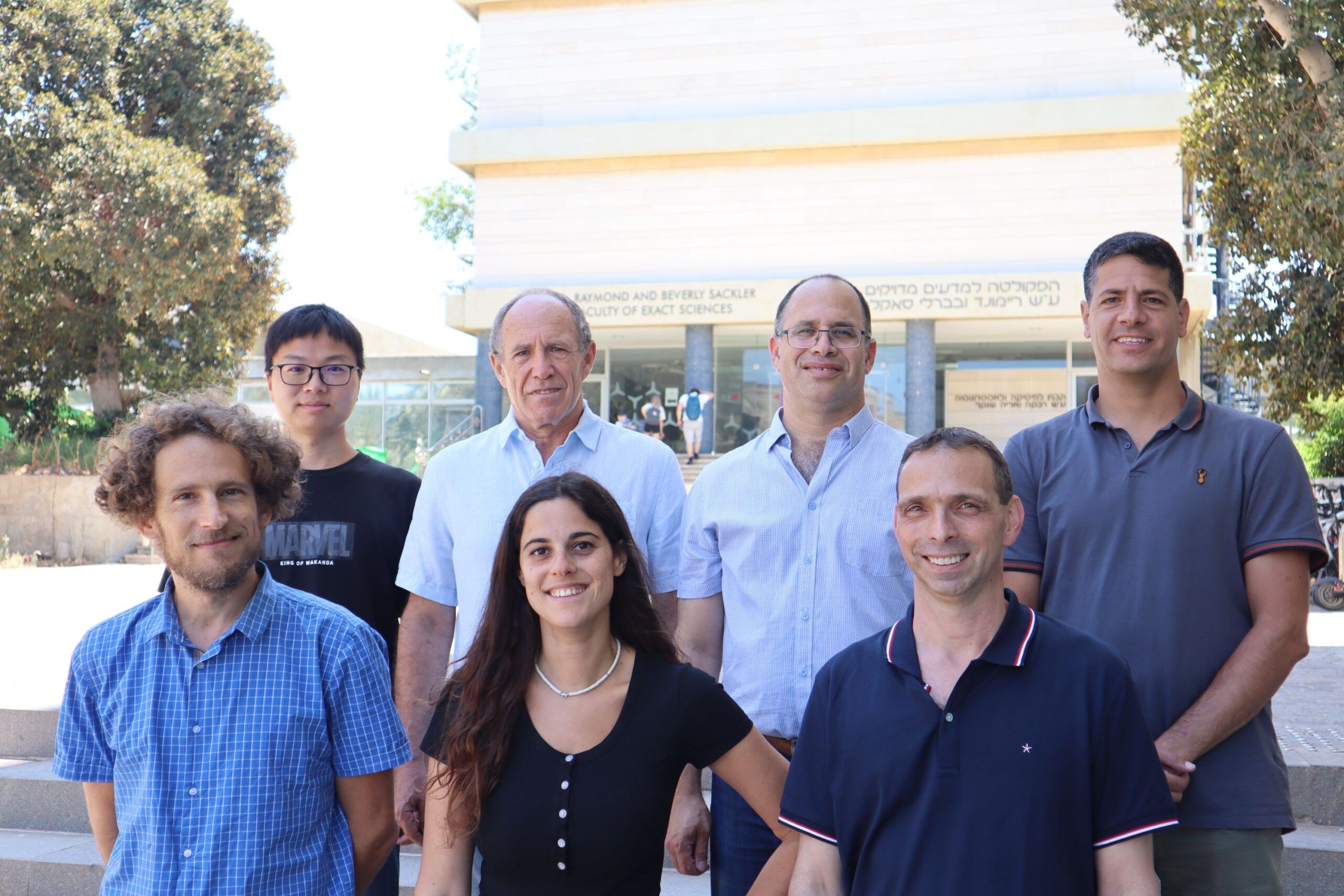
The research team
- The new technology, enabling the storage of information in the thinnest unit known to science, is expected to improve future electronic devices in terms of density, speed, and efficiency.
- The allowed quantum-mechanical electron tunneling through the atomically thin film may boost the information reading process much beyond current technologies.
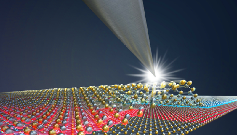
- The technology involves laterally sliding one-atom-thick layers of boron and nitrogen one over the other – a new way to switch electric polarization on/off.
A scientific breakthrough: Researchers from Tel Aviv University have engineered the world’s tiniest technology, with a thickness of only two atoms. According to the researchers, the new technology proposes a way for storing electric information in the thinnest unit known to science, in one of the most stable and inert materials in nature. The allowed quantum-mechanical electron tunneling through the atomically thin film may boost the information reading process much beyond current technologies.
The research was performed by scientists from the Raymond and Beverly Sackler School of Physics and Astronomy and Raymond and Beverly Sackler School of Chemistry. The group includes Maayan Vizner Stern, Yuval Waschitz, Dr. Wei Cao, Dr. Iftach Nevo, Prof. Eran Sela, Prof. Michael Urbakh, Prof. Oded Hod, and Dr. Moshe Ben Shalom. The work is now published in Science magazine.
“Our research stems from curiosity about the behavior of atoms and electrons in solid materials, which has generated many of the technologies supporting our modern way of life,” says Dr. Ben Shalom. “We (and many other scientists) try to understand, predict, and even control the fascinating properties of these particles as they condense into an ordered structure that we call a crystal. At the heart of the computer, for example, lies a tiny crystalline device designed to switch between two states indicating different responses – “yes” or “no”, “up” or “down” etc. Without this dichotomy – it is not possible to encode and process information. The practical challenge is to find a mechanism that would enable switching in a small, fast, and inexpensive device.
Current state-of-the-art devices consist of tiny crystals that contain only about a million atoms (about a hundred atoms in height, width, and thickness) so that a million of these devices can be squeezed about a million times into the area of one coin, with each device switching at a speed of about a million times per second.
Following the technological breakthrough, the researchers were able, for the first time, to reduce the thickness of the crystalline devices to two atoms only. Dr. Ben Shalom emphasizes that such a thin structure enables memories based on the quantum ability of electrons to hop quickly and efficiently through barriers that are just several atoms thick. Thus, it may significantly improve electronic devices in terms of speed, density, and energy consumption.
In the study, the researchers used a two-dimensional material: one-atom-thick layers of boron and nitrogen, arranged in a repetitive hexagonal structure. In their experiment, they were able to break the symmetry of this crystal by artificially assembling two such layers. “In its natural three-dimensional state, this material is made up of a large number of layers placed on top of each other, with each layer rotated 180 degrees relative to its neighbors (antiparallel configuration)” says Dr. Ben Shalom. “In the lab, we were able to artificially stack the layers in a parallel configuration with no rotation, which hypothetically places atoms of the same kind in perfect overlap despite the strong repulsive force between them (resulting from their identical charges). In actual fact, however, the crystal prefers to slide one layer slightly in relation to the other, so that only half of each layer’s atoms are in perfect overlap, and those that do overlap are of opposite charges – while all others are located above or below an empty space – the center of the hexagon. In this artificial stacking configuration the layers are quite distinct from one another. For example, if in the top layer only the boron atoms overlap, in the bottom layer it’s the other way around.”
Dr. Ben Shalom also highlights the work of the theory team, who conducted numerous computer simulations “Together we established deep understanding of why the system’s electrons arrange themselves just as we had measured in the lab. Thanks to this fundamental understanding, we expect fascinating responses in other symmetry-broken layered systems as well,” he says.
Maayan Wizner Stern, the PhD student who led the study, explains: “The symmetry breaking we created in the laboratory, which does not exist in the natural crystal, forces the electric charge to reorganize itself between the layers and generate a tiny internal electrical polarization perpendicular to the layer plane. When we apply an external electric field in the opposite direction the system slides laterally to switch the polarization orientation. The switched polarization remains stable even when the external field is shut down. In this the system is similar to thick three-dimensional ferroelectric systems, which are widely used in technology today.”
“The ability to force a crystalline and electronic arrangement in such a thin system, with unique polarization and inversion properties resulting from the weak Van der Waals forces between the layers, is not limited to the boron and nitrogen crystal,” adds Dr. Ben Shalom. “We expect the same behaviors in many layered crystals with the right symmetry properties. The concept of interlayer sliding as an original and efficient way to control advanced electronic devices is very promising, and we have named it Slide-Tronics”.
Maayan Vizner Stern concludes: “We are excited about discovering what can happen in other states we force upon nature and predict that other structures that couple additional degrees of freedom are possible. We hope that miniaturization and flipping through sliding will improve today’s electronic devices, and moreover, allow other original ways of controlling information in future devices. In addition to computer devices, we expect that this technology will contribute to detectors, energy storage and conversion, interaction with light, etc. Our challenge, as we see it, is to discover more crystals with new and slippery degrees of freedom.”
The study was funded through support from the European Research Council (ERC starting grant), the Israel Science Foundation (ISF), and the Ministry of Science and Technology (MOST).

